Internship
Deep investigation of GaN/dielectrics gate stack through ab-initio simulation.
Domaine: Microelectronics, Solid state physics, Ab-initio simulation
Contract type: Internship, Starting date: 01/02/2023 (please send application as soon as possible but not later than 30/11/2022)
Title: Deep investigation of GaN/dielectrics gate stack through ab-initio simulation
Internship description:
MOS-HEMT devices have erased a lot of interest in the state of art and specifically for compact and high power density applications. Thanks to the presence of a high two-dimensional gas electron (2DEG) at the AlGaN/GaN heterojunction and the very promising thermal resistance and high electron mobility in GaN, these transistors are capable of supporting high currents densities.
The MOS-HEMT Gate stack (GaN/dielectrics), one the most crucial technology development, is defined by the threshold voltage (Vth) and the stability of this voltage under stress conditions (ΔVth). NORMALLY-OFF (Vth>0) and reliable transistors (ΔVth=0) are highly desired in systems applications. Unfortunately, MOS-HEMT transistors still suffer of both Fermi level pinning at undesired traps and uncontrolled Vth dynamic under blocking stress. Computer modeling and simulations can help understand the phenomena inside devices. First principles (ab initio) calculations, including the widely used density functional theory (DFT), are particularly useful for studying phenomena at the microscopic level.
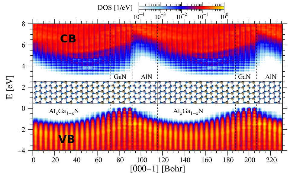
This method allows to predict the properties of atomic and molecular systems only on the basis of the knowledge of their chemical composition. Using DFT calculations, the properties of the near interface area will be investigated, in particular the shape and shift of the energy bands, the location of the Fermi level, the interface states and the distribution of the trap density. These parameters are fundamental for explaining the pinning and dynamic Vth behaviors. Correlation between simulations and experimental results will be carried out during this study. Surface characterization data will be obtained from several measurement techniques such as AFM, HRTEM, EDX, HAXPES, XRR and TOF-SIM, giving access to the chemical composition and structural properties of the subsurface area of the GaN/dielectric stack.
Methodologies/Tool: density functional theory (DFT) calculations and electrical/physical characterizations.
Candidate: Master preferable in Electronics or Solid-State Physics, although general background in physics / mathematics / computer science is fine. Proficiency in topics related to "Internship description" is not necessary, the candidate is supposed to learn the details during the internship (enthusiasm and willingness to learn is obligatory).
Site: Grenoble, Le Commissariat à l'énergie atomique et aux énergies alternatives (CEA) Collaboration with the Institute oh High Pressure Physics of the Polish Academy of Sciences (IHPP PAS), Warsaw, Poland will be established. This institute is an internationally recognized center for the growth of bulk, GaN crystals (by amonothermal method) for native GaN substrates, epitaxial quantum structures (MOVPE and MBE) as well as optoelectronic and electronic devices based on III-nitrides semiconductors.
Location: France, Auvergne-Rhône-Alpes, Isère (38)
Language: English or French + Polish
Contract duration (months): 6 months
PhD opportunity after internship: yes
Salary: Internship salary: ~700 EUR + allowances to accommodation, tickets, etc. Estimated PhD salary: 1300-1600 EUR + allowances
Contact: Lukasz.Borowik@cea.fr, pkempisty@unipress.waw.pl


